Welcome to sysilicon.com


Si-Si bond
When the epitaxial layer thickness is more than 50 um, the silicon-silicon bonded wafer has a better cost advantage.
For high voltage devices, such as MOSFET and IGBT is feasible alternative materials.
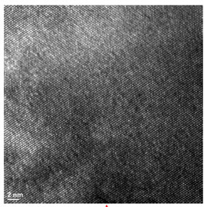
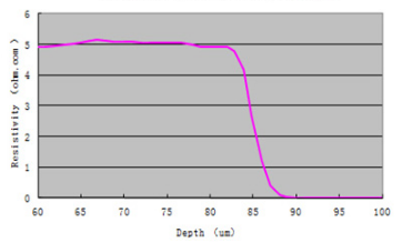
Good TEM and SRP test results ensure the quality of silicon-silicon bonded wafers.
Address: No. 15-22, hunnan Road, Shenyang Export Processing Zone, Liaoning